


Imaging Photometer Value
Future Trends in Imaging Photometry and What to Expect Next
Improved low-noise sensor design will push minimum detectable brightness even lower, expanding capability for ultra-dark display testing. For manufacturers, staying competitive means partnering with suppliers who invest in ongoing R&D and can upgrade both hardware and software as requirements evolve. Choosing a forward-thinking supplier today ensures your optical measurement infrastructure remains capable and cost-effective as display and lighting technologies advance over the coming decade.
Customization Options




Product Overview
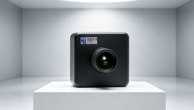
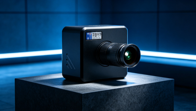
Understanding Dynamic Range in Imaging Luminance Meters and Why It Matters
Key Factors for Selecting the Right Lens for Your Luminance Meter Setup
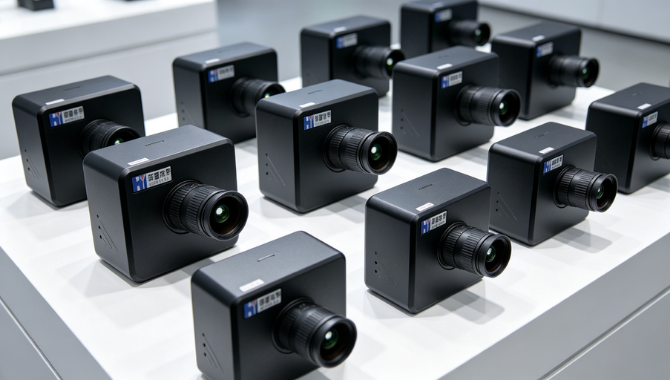
Cost Benefits of CMOS Imaging Luminance Meters for Mid-Size Manufacturers
For mid-size manufacturers adding optical measurement capability, CMOS-based imaging luminance meters offer compelling cost advantages over traditional scanning photometer systems. The core CMOS sensor technology benefits from enormous economies of scale driven by the consumer camera and smartphone industries, dramatically reducing component costs compared to specialized scientific-grade detectors. This translates into purchase prices often significantly lower than legacy scanning systems, without sacrificing the accuracy needed for most production quality control applications. Beyond upfront cost, CMOS imaging systems have no moving mechanical parts, cutting maintenance requirements and extending service life considerably. For companies producing display modules, backlights or automotive lighting components at mid-range volumes, CMOS imaging luminance meters deliver professional-grade measurement performance at an accessible price point. This affordability enables smaller manufacturers to implement 100% optical inspection rather than relying on manual visual sampling, directly improving product quality and reducing downstream warranty and return costs.
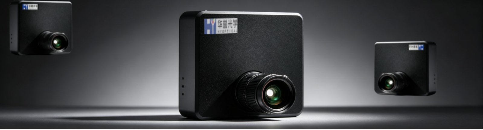
Product Specifications & Parameters
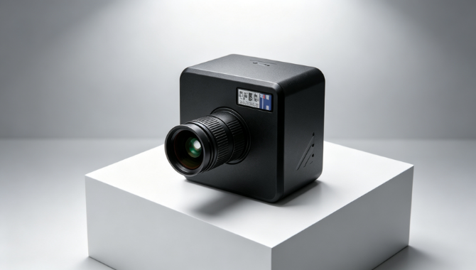
| Specification | HY020Y 206m |
| Detector Model, Diagonal Size, Pixel Size | Sony IMX183, 16mm, 2.4μm |
| Detector Type | 8bit / 10bit / 12bit CMOS |
| Pixel Array | 5472 × 3648 |
| Dynamic Range | 65.5dB |
| High Dynamic Range (HDR) | >1,000,000:1 |
| Minimum Luminance (cd/m², SNR=41.5dB) | 0.01 |
| Maximum Standard Luminance (cd/m²) | 50000 |
| Maximum Luminance with ND Filter (cd/m²) | 1,000,000 |
| System Accuracy | Luminance(Y) ±3% |
| Short-Term Repeatability | Luminance(Y) ±0.1% |
| Standard Lenses & Field of View (H×V) | 16mm: 31°×23° 25mm: 32°×24° 50mm: 16°×12° |
| Minimum Measuring Time (100cd/m² Native) | Luminance: 3s |
| Spatial Measurement Functions | Luminance, Uniformity, Customizable Parameters |
| Output Unit | cd/㎡ |
| Communication Interface | GigE Ethernet |
| Power Consumption | 2.4W @12VDC |
| Dimension (H×W×D) | 90mm × 100mm × 137mm |
| Operating Temperature | -30℃ ~ 60℃ |
| Operating Humidity | 20% ~ 95% RH, non-condensing |
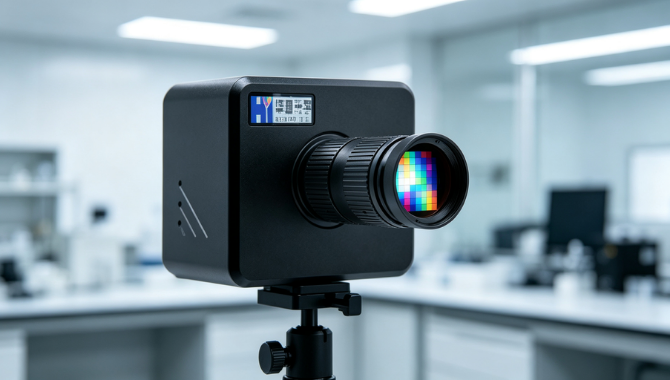
HY owns core calibration algorithms for imaging luminance meters, with all flat-field correction, linearity correction and brightness calibration models developed in-house. Each unit undergoes multiple standard light source calibrations before shipment, ensuring accurate, traceable measurements. Our team continuously optimizes algorithms and quickly develops custom measurement functions for special needs.
Application Fields & Scenarios


 Tiếng Việt
  English
  Русский
  Español
  Français
  Português